Spherical aberration-corrected transmission electron microscope (JEM-2200FS)
Spatial resolution 0.1 nm (after aberration correction)
Accelerating voltage 200 kV
Electron beam spectrometer Ω-type filter / Energy resolution 0.8 eV
Spherical aberration-corrected transmission electron microscope (JEM-2200FS)
CCD Camera 2048×2048 pixel
Aberration correction device CEOS Cs correction device (for TEM mode)
Features: Measurement in both TEM/STEM modes is possible. This general-purpose analytical electron microscope can use various types of sample holders, such as sample heating and cryogenic holders.
Kyoto University
Use -by-the-hour Technical Agencies Technical Assistance
You must release a result
Other Research Institutes
Use -by-the-hour Technical Agencies Technical Assistance
You must release a result
Companies, etc.
Use -by-the-hour Technical Agencies Technical Assistance
You must release a result
Users are requested to submit their samples, and our technical staff will conduct the measurements.
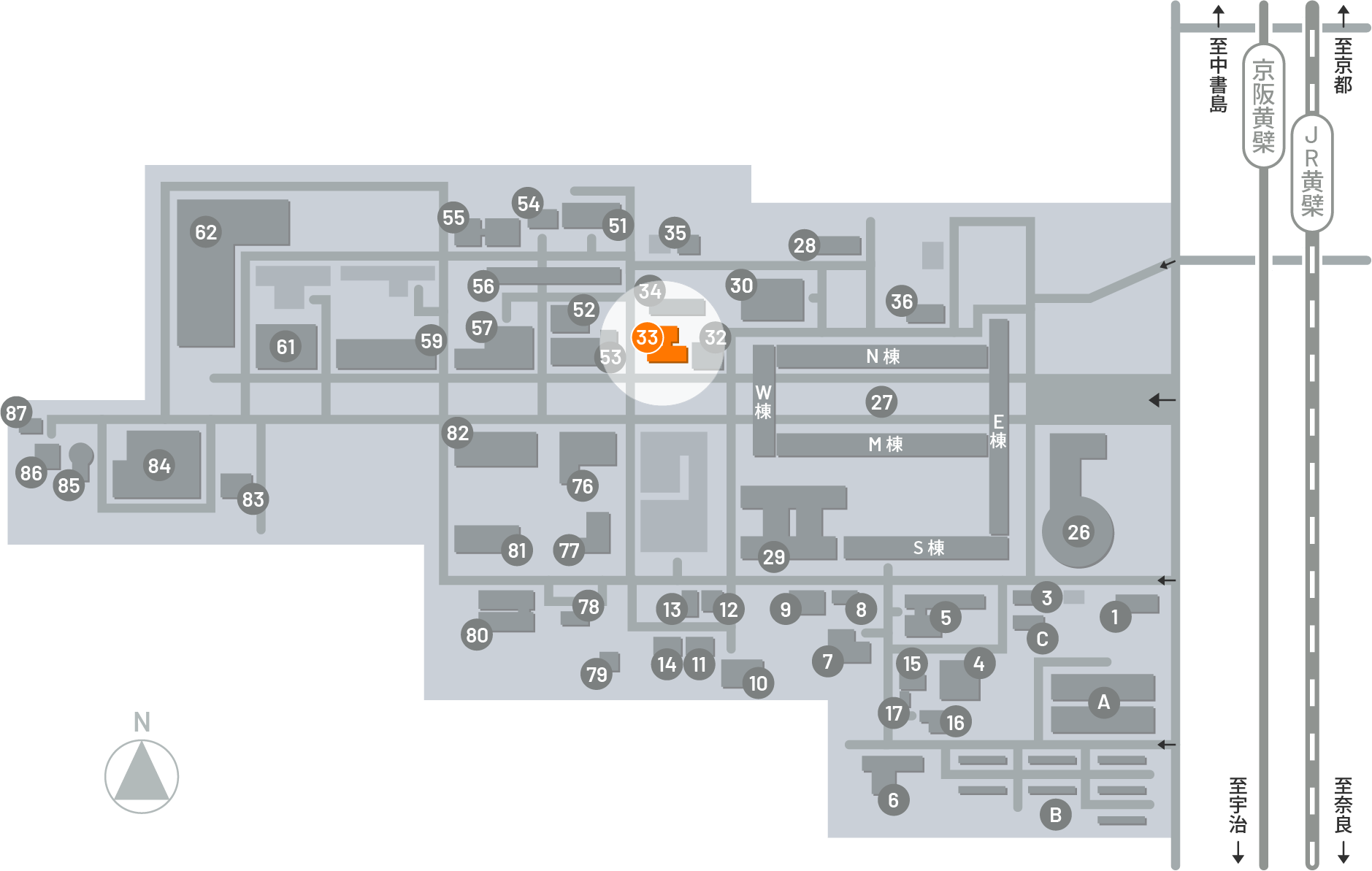
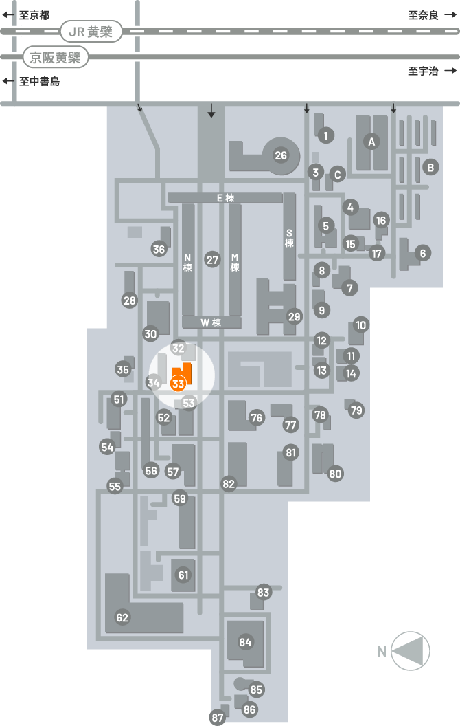
Division of Electron Microscopy and Crystal Chemistry,Institute for Chemical Research
(Contact:Kiyomura)
MAIL:arim*eels.kuicr.kyoto-u.ac.jp
※Please change 「*」 to 「@」 and send.

