Marcus-type high-frequency glow discharge surface analyzer (GDS) GD-Profiler
Rapid surface analysis and surface analysis of non-conductive materials are also possible.
Pulse sputtering (patented) enables low-damage, high-resolution measurements.
It can be used as a pretreatment and etching machine for microscopic observation.
Bulk analysis (quantitative analysis of solid materials) is also possible.
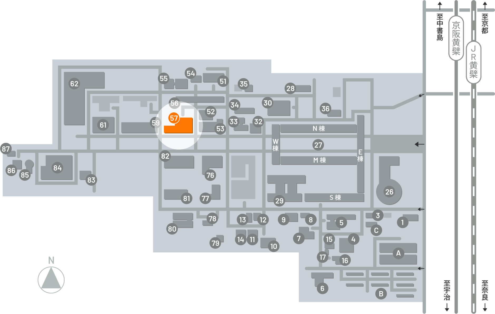
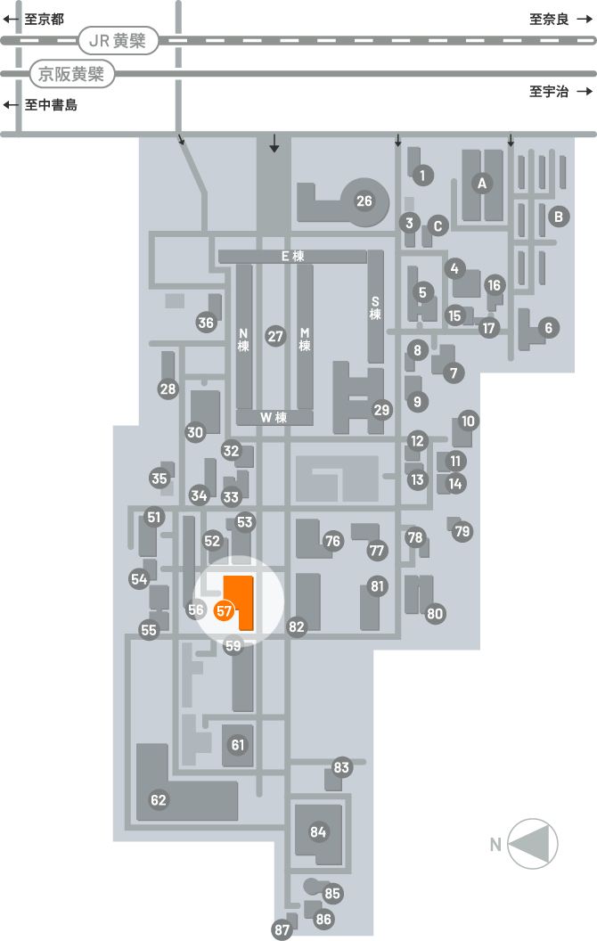
Installation Location 57 North Building 2 (partially located in the DuET experiment building in North Building 1)
Kyoto University
Use -by-the-hour
Accepted only between 9 am and 5 pm off campus
Other Research Institutes
Use -by-the-hour
Accepted only between 9 am and 5 pm off campus
Companies, etc.
Public offering
Person of Kyoto University:Please contact the person in charge.
Others:Project Zero Emission Energy Research Please contact the person in charge.((Paid use and use under a joint research agreement are available.)
※ For details on how to apply, please refer to the device’s website.
http://www.iae.kyoto-u.ac.jp/zero_emission/
Advanced Energy Conversion Division Advanced Energy Structural Materials Research Section(Contact:Omura)
TEL:0774-38-3568
MAIL:muster-office*iae.kyoto-u.ac.jp
※Please change 「*」 to 「@」 and send.