Ion milling device for FIB post-processing NanoMill Model1040
This is a milling device for post-processing TEM samples prepared using FIB (focused ion beams). When preparing samples using FIB, the surface layer often becomes amorphous or gallium is implanted, and such damaged layers can be 10 to 30 nm thick.
NanoMill is the ideal device for removing this kind of damaged layer.
An image of the sample is acquired using a SED (secondary electron detector), and ions can be milled to only the desired spot, thereby preventing re-deposition.
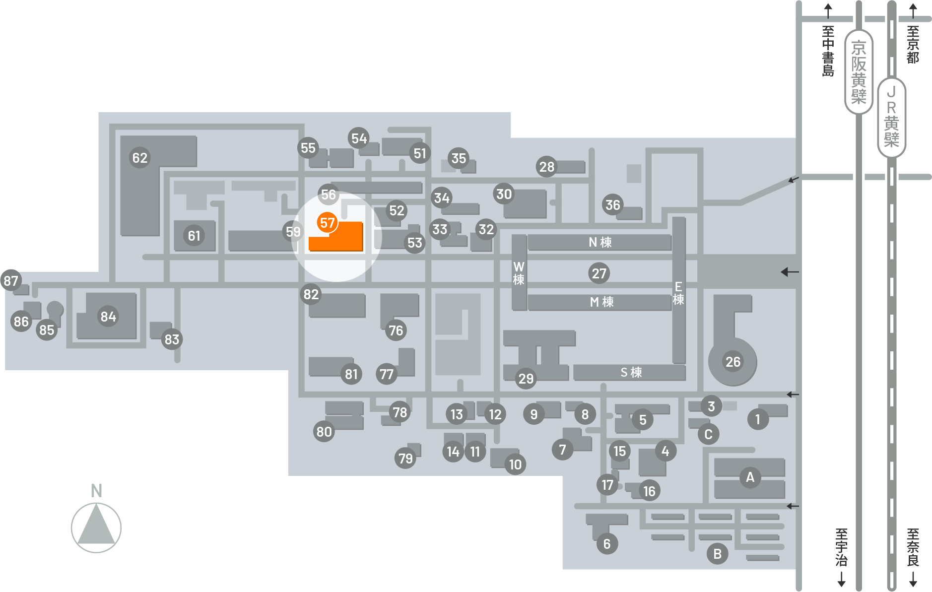
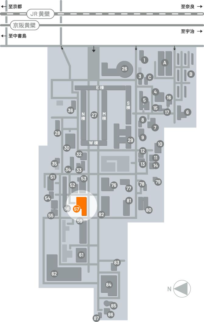
Installation Location 57 North Building 2 (partially located in the DuET experiment building in North Building 1)
Kyoto University
Use -by-the-hour
Accepted only between 9 am and 5 pm off campus
Other Research Institutes
Use -by-the-hour
Accepted only between 9 am and 5 pm off campus
Companies, etc.
Public offering
Person of Kyoto University:Please contact the person in charge.
Others:Project Zero Emission Energy Research Please contact the person in charge.((Paid use and use under a joint research agreement are available.)
※ For details on how to apply, please refer to the device’s website.
http://www.iae.kyoto-u.ac.jp/zero_emission/
Advanced Energy Conversion Division Advanced Energy Structural Materials Research Section(Contact:Omura)
TEL
0774-38-3568
MAIL
ohmura.takamasa.2r*kyoto-u.ac.jp
※Please change 「*」 to 「@」 and send.