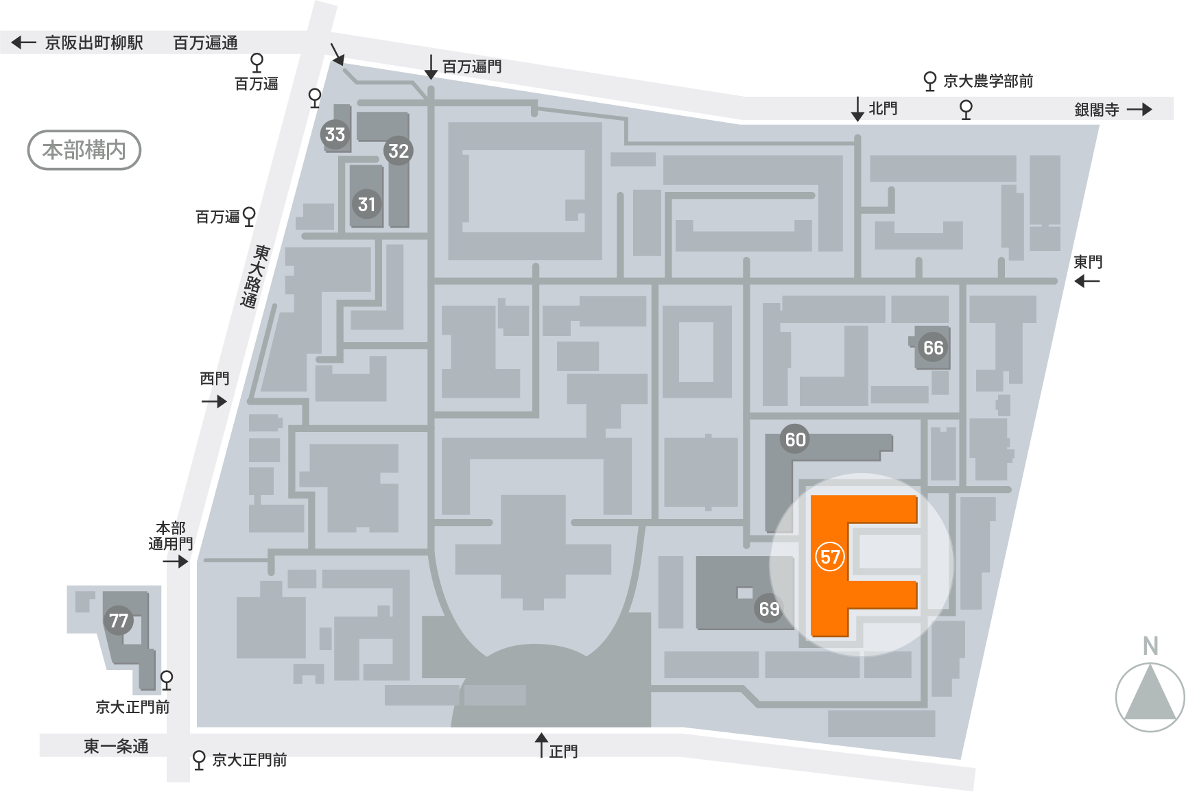
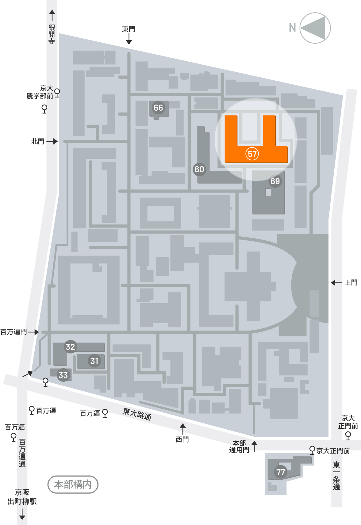
Transmission electron microscope JEM-2010
It is a conventional transmission electron microscope (TEM). The CCD camera is side-mounted, which is not suitable for acquiring high-resolution images. An ion milling device for TEM sample preparation is also available for use.
Materials Sciences and Engineering Department
(1) Individuals who belong to a department or the Materials Science Course in the Department of Physics and Engineering in Kyoto University (hereinafter referred to as “the university”).
(2) Faculty or students of Kyoto University who belong to departments or courses other than the specified one.
(3) Individuals affiliated with national or local government bodies, national university corporations or university joint-use institutions, independent administrative institutions, or corporations or organizations engaged in educational or research activities.
(4) Individuals engaged in research and development activities in companies or other organizations.
(5) Other individuals deemed appropriate by the responsible manager.
The reservation is available up to 2 weeks in advance, and within that range, each person can only reserve one time slot.
Materials Sciences and Engineering Department
Kenji Kazumi
075-753-5474
kazumi.kenji.6r*kyoto-u.ac.jp
※Please change 「*」 to 「@」 and send.

