
light exposure equipment DL-1000KIR
Model
DL-1000KIR
Manufacturer
Nano System Solutions Co., Ltd.
Specification
Location
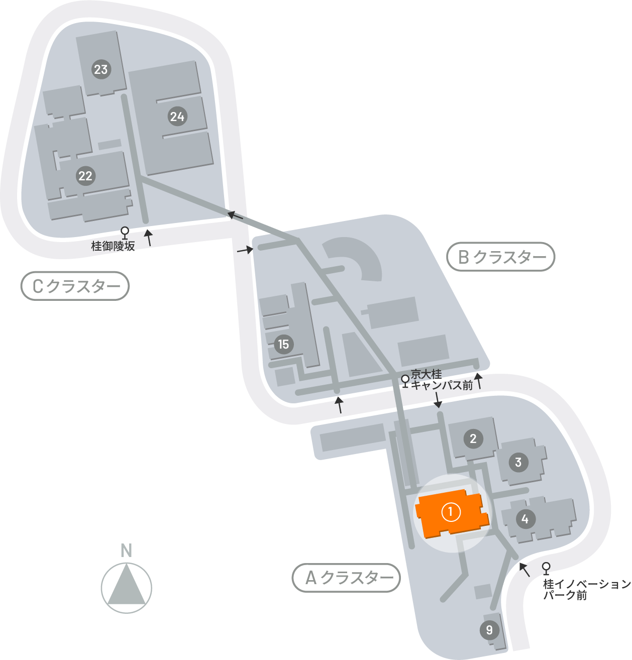
Katsura Campus, Building A1 1st floor, Room 102
Installation Year
2021
Overview
High-precision and high-resolution photolithography without the need for masks is possible.
Responsible department
Electronic Science and Engineering Department
Photonics and Electronics Science and Engineering Center
Photonics and Electronics Science and Engineering Center
Available Users
(1) Individuals who are faculty members or students of Kyoto University (hereinafter referred to as "the University") and are engaged in research and development related to photonic crystal surface-emitting lasers for the purpose of such research and development.
(2) Individuals who are faculty members or students of the University, excluding those mentioned in the preceding item, and are engaged in research and development related to photonic crystal surface-emitting lasers for the purpose of such research and development.
(3) Individuals affiliated with a country, local government entity, national university corporation, university joint-use institution corporation, independent administrative corporation, or a legal entity or organization that conducts education and research as its business purpose, and are engaged in research and development related to photonic crystal surface-emitting lasers for the purpose of such research and development.
(4) Individuals engaged in research and development in companies or other organizations for the purpose of research and development related to photonic crystal surface-emitting lasers.
(5) Any other individuals deemed appropriate by the person in charge of management.
Notes
Usage rules
Inquiries
Electronic Science and Engineering Department
Masahiro Yoshida
075-383-7109
yoshida.masahiro.4n*kyoto-u.ac.jp
※Please change 「*」 to 「@」 and send.
Masahiro Yoshida
075-383-7109
yoshida.masahiro.4n*kyoto-u.ac.jp
※Please change 「*」 to 「@」 and send.