Ultra-low accelerating voltage field emission scanning electron microscope (FE-SEM (ULTRA55))
FE-SEM observation allows observation at a higher magnification than a scanning electron microscopy (SEM). This enables observation of surface irregularities, composition distribution, crystal particles, etc., and crystal orientation analysis using EBSD.
Elemental analysis can also be performed using the energy-dispersive X-ray analyzer (EDX) attached to the FE-SEM.
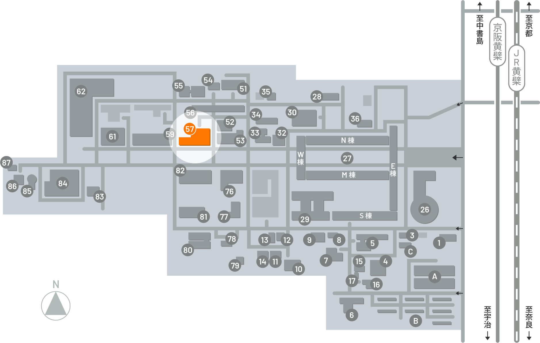
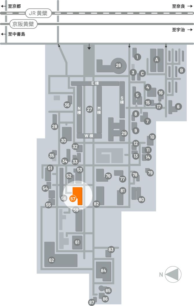
Installation Location 57 North Building 2 (partially located in the DuET experiment building in North Building 1)
Kyoto University
Use -by-the-hour
Accepted only between 9 am and 5 pm off campus
Other Research Institutes
Use -by-the-hour
Accepted only between 9 am and 5 pm off campus
Companies, etc.
Public offering
Person of Kyoto University:Please contact the person in charge.
Others:Project Zero Emission Energy Research Please contact the person in charge.((Paid use and use under a joint research agreement are available.)
※ For details on how to apply, please refer to the device’s website.
https://www.iae.kyoto-u.ac.jp/center/images/kikiyoukou.pdf
Advanced Energy Conversion Division Advanced Energy Structural Materials Research Section(Contact:Omura)
TEL:0774-38-3568
MAIL:muster-office*iae.kyoto-u.ac.jp
※Please change 「*」 to 「@」 and send.